
Computer Science
Computing History Displays: Fourth Floor - Computer Circuit Packaging
The main technologies from which computer are built – logic circuits, high-speed memory and hard disk – have improved spectacularly over the years. They are all more than a billion times better in speed/cost from when first introduced. The ways that these components are packaged has necessarily enjoyed an interesting, though less well-known, history of improvement.
With the very first computers the components were connected together with signal-carrying copper wires in an ad-hoc manner. However, in order to use large numbers of components at a reasonable cost, it was quickly found to be necessary to group components into standard packages or modules with multiple copies of each type of module being used. Modules were often imposed at more than one level – there were basic components connected together in modules of a standard shape and form, then these modules treated as components in a second level of packaging. The boundaries between these levels of packaging shifted over time with the shrinkage of component size and the increase in the number of components in a module.
As it has evolved, circuit packaging has faced some continual challenges:
- Cooling - how to remove heat from the active components
- I/O - how to bring signal wires in and out of the package to pins to connect with the next level of packaging
- Wiring – how to connect the components together within the package
Cooling
This was a need evident from the start when logic components (we will use the term gates) were constructed from thermionic valves or tubes, each of which contained a little heating element used to generate electrons. Later, with transistors, there was much less heat per element generated by the switching of logic elements and resistance. But, in order to put elements close together so as to reduce signal delay, cooling continued to be a problem for the most powerful computers. Heat is removed through conduction to surfaces cooled using chilled air or, for the fastest technologies, chilled fluid, usually water.
I/O
It was discovered empirically that the number of I/Os required by any package rises at some power, less than one, of the number of gates in the package. This is known as “Rent’s Rule.” It is not a law of nature because computer designers will use however many I/Os are provided – rather it is the number of I/O that allows designers to feel comfortable that they are not forced to make costly or speed-reducing decisions (for example, not being able to use all of the gates provided in a package, or having to transfer a long word serially in two sections.)
Suppose, for argument, that the number of I/O needed increases by the square root of the number of gates. If an array of 100 (10x10) gates requires 40 I/O around the edge then 10,000 gates (100 x 100) should need 400 I/O. This seems nice and balanced at any given time. However, over time, the size of the components has also decreased exponentially so that the 400 I/O need to fit in almost the same space as the 40. It is often impractical to continue to make I/O pins smaller. The solution that has to be embraced is to spread I/O pins as a 2 dimensional array, rather than being restricted to the edge of the package.
Wiring
If all I/O from components are to be used then the number of interconnections required must increase with the number of components, whether they are gates or themselves modules. So, using the same example as above, going from a module of 10x10 gates to 100 x100 would require the connections within the module to increase by a factor of 100 and the connections between modules by 10 times. The problem of providing enough interconnections is eased somewhat by the shorter local connections being the most frequent.
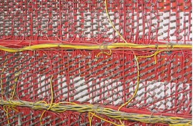
CSIRAC Wiring
Here is some discussion as to how packaging has developed, using examples mainly from our collection.
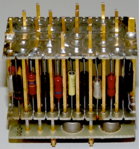
IBM650 Gate
The very first computers were constructed in a fairly ad-hoc fashion. The image just above is the wiring between gates as used in the CSIRAC computer, one of the world's first, housed in the Museum of Victoria, Melbourne.
Ferranti Pegasus Board
However, even the first production computers in the 1950s used packages to construct a gate or small groups of gates. We have examples of modules from the IBM 650 and the Ferranti Pegasus. Wiring connections both within and between modules were still hand-soldered copper wire.
IBM 1620 Circuit Boards
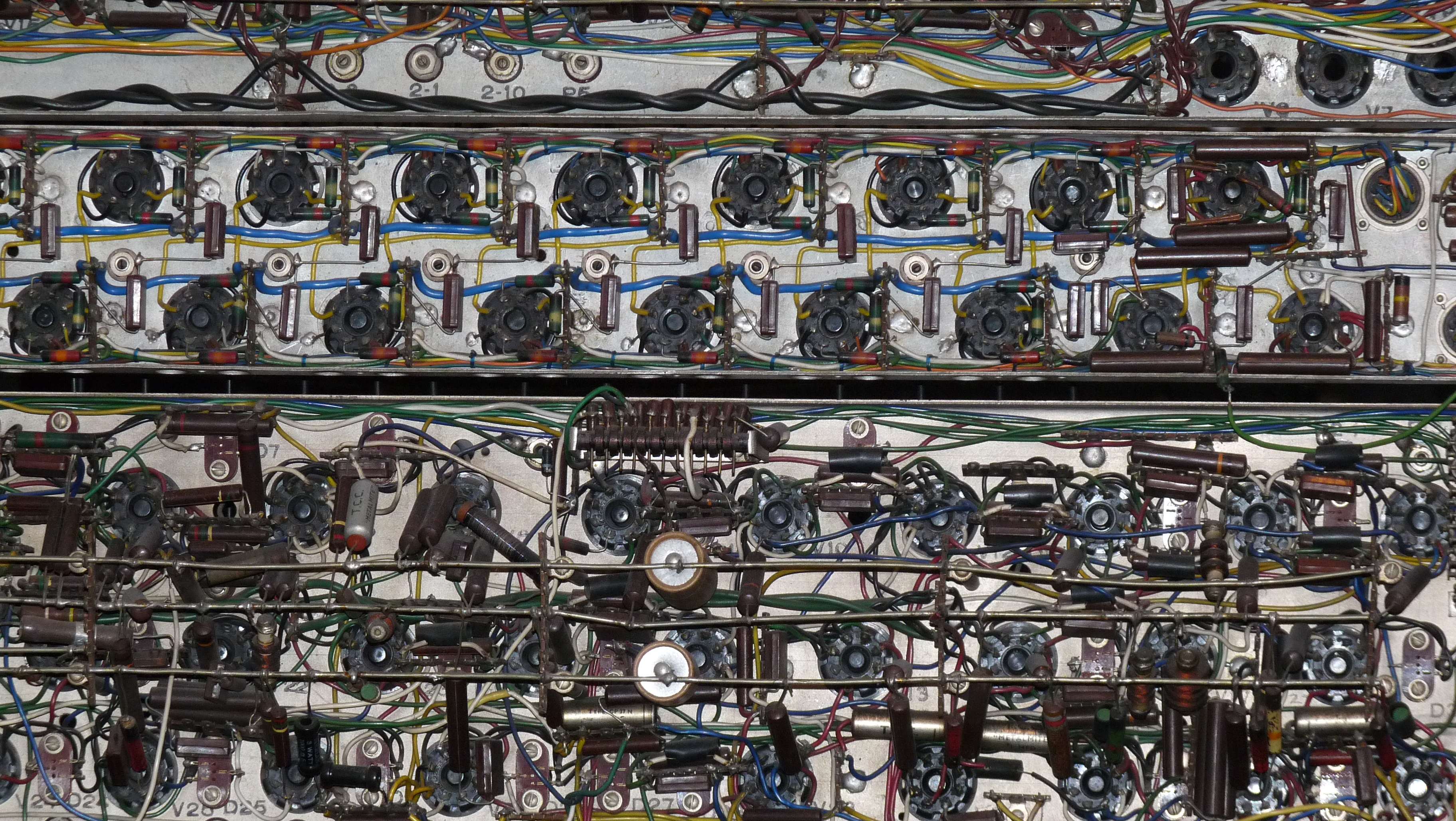
With the move to transistors, the size of circuit elements became much smaller but computers tended to use many more components so modularization became more important. We began to see the use of plastic cards (PCBs - Printed Circuit Boards) with wiring screen-printed, initially on one side only, as in the IBM internal standard SMS (standard modular system) cards as used from the late 1950s – the examples above are from the IBM 1620.
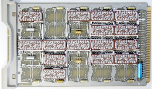
Burroughs Package
Elliott 503 Board
There were many ingenious schemes for packaging developed. We have examples from Burroughs and the CDC 6600 where there were components placed between two boards. The Elliott Automation packaging used two levels of printed board. Connections between boards were still using wires but special machines were designed to wire-wrap back planes under programmed control as with the IBM 1620.
IBM 1620 Back Plane Wiring
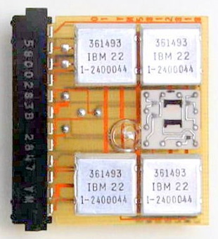
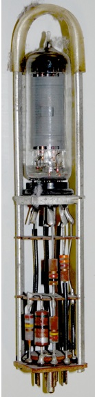
IBM SLT Packaging
From the mid-1960s, integrated circuits started to be developed, with only a few gates per chip to start with. IBM 360’s Solid Logic Technology (SLT) had minimal chips containing just one transistor (the image to the right has the cover removed from one SLT package, showing the contents). However, they also developed a ceramic module to carry the chips, initially with just one layer of wiring. SLT used solder bumps on the surface of the chip to make connections to the ceramic module – this was the start of a line of development that continued up until the present. The chip packages were in turn mounted on PCBs that began to have multiple levels of wiring internally. The printed layers were connected, where necessary, by drilling holes called “vias” between all layers and plating the inside of the holes with conducting metal.
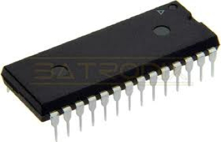
DIP-mounted chip
The more-conventional method of mounting small chips was for the chip to include (relatively) large pads around its edges. The chip was mounted inside a chip carrier with tiny signal wires bonded from the chip surface to connectors on the chip carrier. For conventional chips the standard chip carrier was the DIP package (Dual-in-Line Package). Chips in DIPs could be mounted by being soldered directly on a PCB or inserted in-turn into carriers soldered to the boards.
Sometimes a second level of PCB was used to plug-in smaller PCBs. However, direct wiring was still common with faster computers.
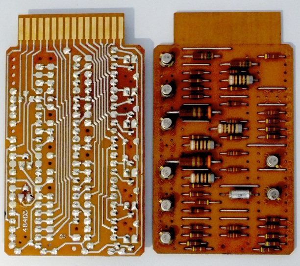
Medium Density chips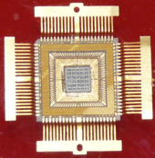
Chip Carrier
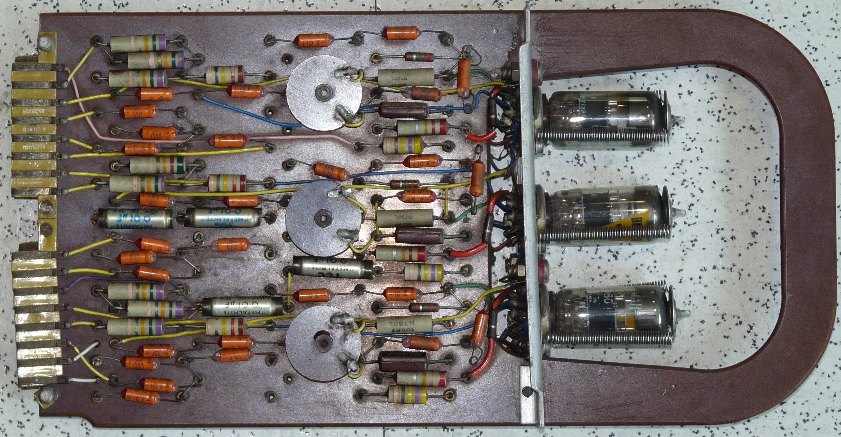
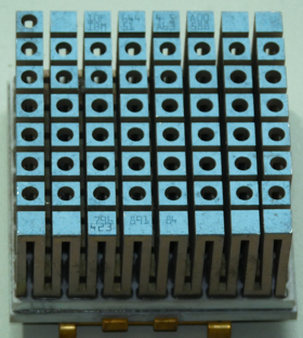
Amdahl 470 MCC
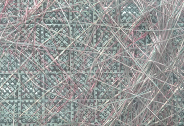
By the mid 1970s computers were beginning to use chips with 100 to 1000 gates. This has the effect of making it very difficult to have multiple copies of any chips – most chips were unique - many 100s of chip-types could be needed. This problem was handled by chips being arrays of gates that were the same apart from wiring layers. Multiple layers of wiring had to be used, both on chip and within the boards on which the chips were mounted. The Amdahl 470 is an interesting example. The chips had 100 gates and 40 I/O pins – the chips were connected using fine wires to the chip carrier. Heat was removed from the back of each chip using an air-cooled stud. The multi-chip carriers (MCCs) of 121 chips had 12 layers of wiring but much point-to-point “manual” wiring was required. Connections between MCCs in a processor frame were still point-to-point – another rats-nest of wires.
Wiring on back of MCC
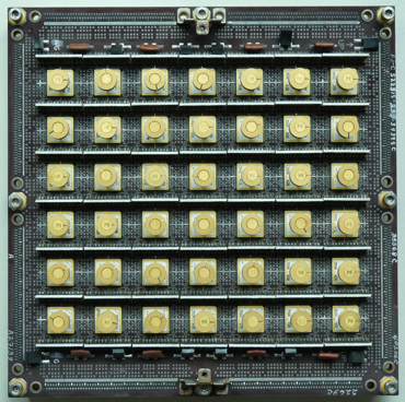
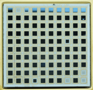
The later IBM 3081 used chips with 704 gates. The chips had an 11 x 11 (121) array of solder bumps and were mounted face down (flip chip configuration) on a 90 mm square ceramic module having 33 layers of wiring, 100 chips per module. These ceramic modules have an array of 1800 pins on the rear and are mounted in-turn on PCBs with 20 layers of internal wiring, thus eliminating the need for discrete wiring between boards.
The 3081 ceramic boards were held in a TCM (Thermal Conduction Module). Metal spring-loaded pins made contact with the back of each chip and conducted heat to a water-cooled plate – the whole module was immersed in Helium, being a better conductor of heat than air.
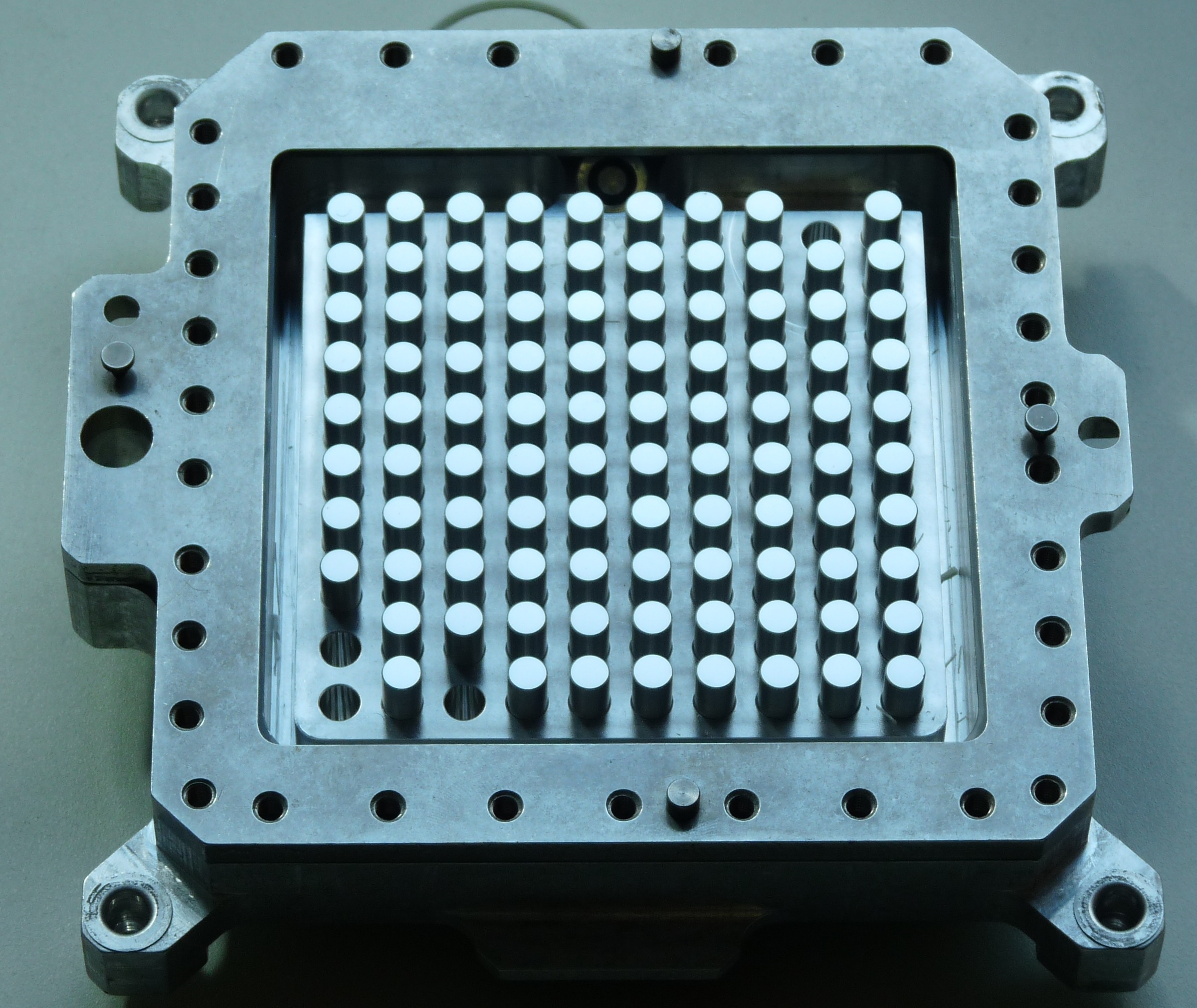
Spring-loaded fingers for cooling
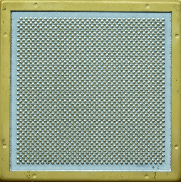
Chips on TCM ceramic board
Pins on back of TCM
Chips of the same density and similar ceramic packages were used in the IBM 4381 which featured a air-cooled heat-sink of novel design.
4381 Heat Sink
As density improved, the problems of packaging were somewhat eased - eventually a whole computer processor was just one chip. However, the pressure for providing interconnections between gates on each chip and between chips continued to be severe, in line with Rent’s rule. There may have been fewer chips to deal with but the heat from each chip became a limiting factor. High-density chips in general use are characterized by very large and fancy heat-sinks. Here is one, about 10cm x 15cm, for a single microprocessor.
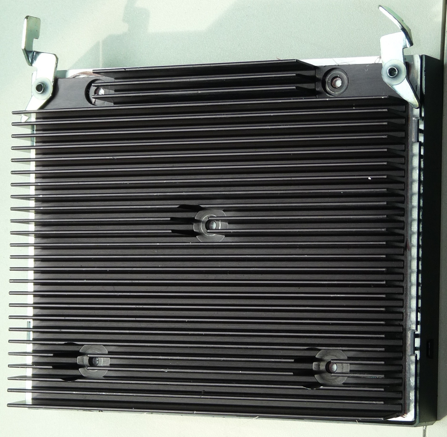
Large Heat Sink
The chips tend to be held flip-chip on ceramic carriers which are connected to boards with a 2-D array of pins. Here we have an example of an Intel chip mounted on a ceramic chip carrier with an array of pins, shown next to the socket mounted on a PCB.
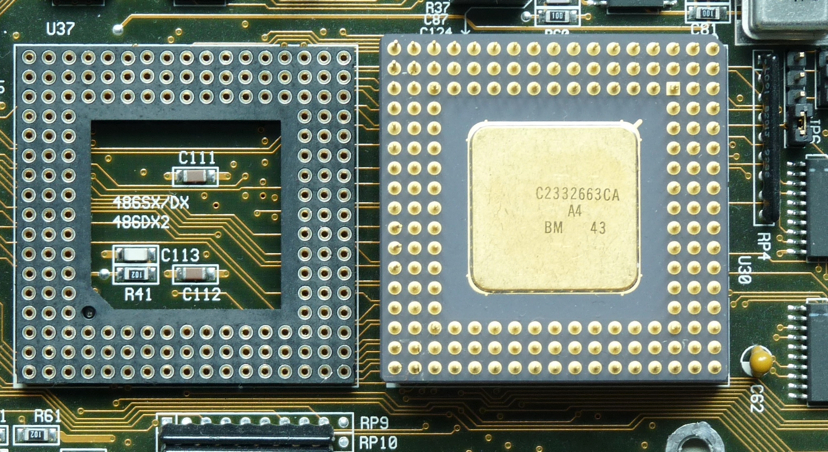
Intel High-density Chip

